Moe L @lioumo
Taiwan Joined April 2014-
Tweets40
-
Followers5
-
Following67
-
Likes2K

大家以為 NVIDIA 只是要把交換器的光模組換成 CPO,其實真正要換光的是 GPU 跟 GPU 之間的 NVLink。 NVIDIA 跟思科一起推插拔式的 USFP,單通道 400G,一個模組 6.4T。那條線是櫃跟櫃之間的網路,插拔式不會死。 這次 Ian Buck 在 OCP 講的是另一條線:現在一櫃 72 顆 GPU 連成一台,他說明年要做到 576 顆,理由是 10 兆參數的模型一櫃已經裝不下。 72 到 576 是 8 倍。銅線就像延長線,房間裡很好用,拉到隔壁棟就不行了。 所以會有兩條光:對外的網路走插拔式,對內的 NVLink 走 CPO。雷射跟光纖對準的需求是兩邊加起來,不是一邊取代另一邊。 數字是 NVIDIA 喊的,雷射是 Lumentum 要生出來的。
CPO 一來,光模組就死了。 這週 OCP 上,推 CPO 最兇的輝達,反而和思科一起發表了一個新的插拔式光模組規格:USFP。 規格是每通道 400G。第一代 16 通道,放在和現在 OSFP 差不多大的空間裡;思科部落格寫明,16 通道是 6.4T,未來擴到 32 通道是 12.8T。 網路上「6.4T 還是

That’s why we had to cut RAM in half for Optimus lol.😂
@Bqlsj2023 “This is why RAM is so expensive” 🤣🤣

英伟达上周又历史新高了 我看B站除了好多恶搞视频 不得不说,现在Ai做视频,基本看不出来痕迹 太夸张了

Someone used Claude Opus 5.5 to make a 3D animation of Nvidia Blackwell GPUs (from server down to an atom). Took 1 hour and full animation “runs from single HTML file, directly in browser. No vid editor. No pre-rendered 3D sequence. Just browser-based experience.” Very cool.
Starship Flight 14, the first morning launch from Starbase since Flight 5
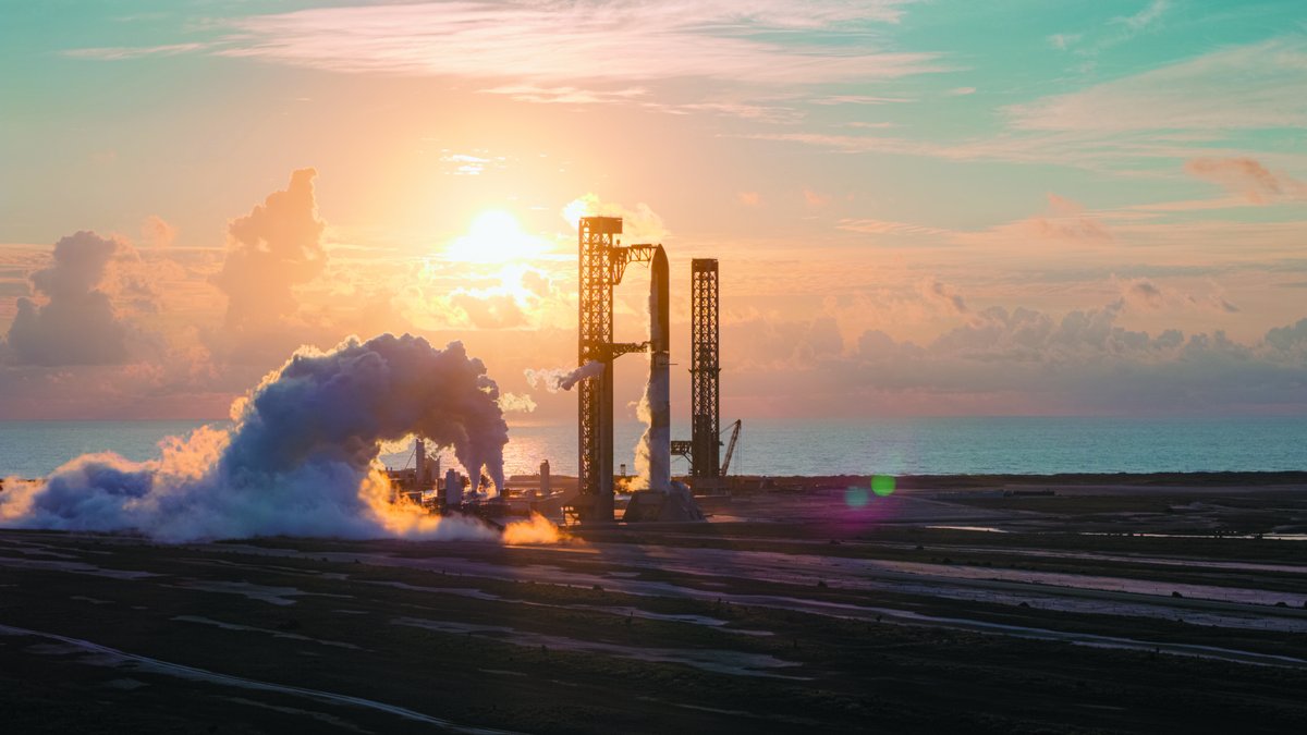
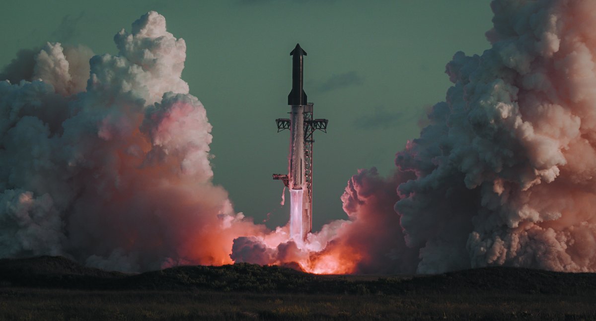
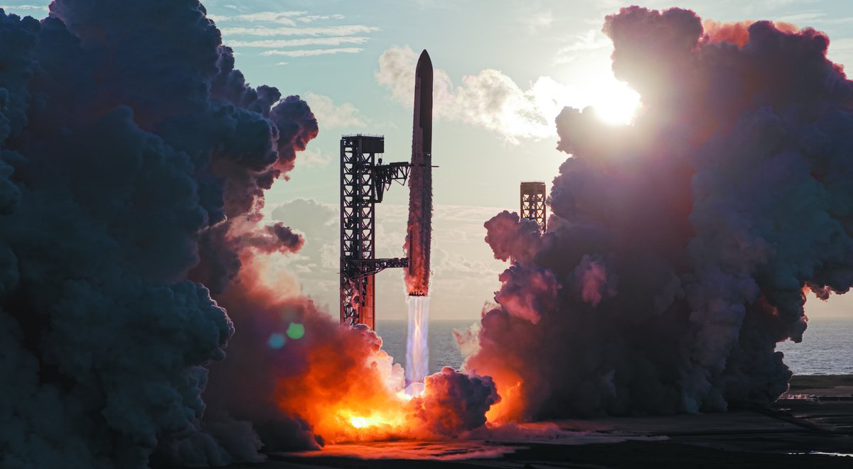
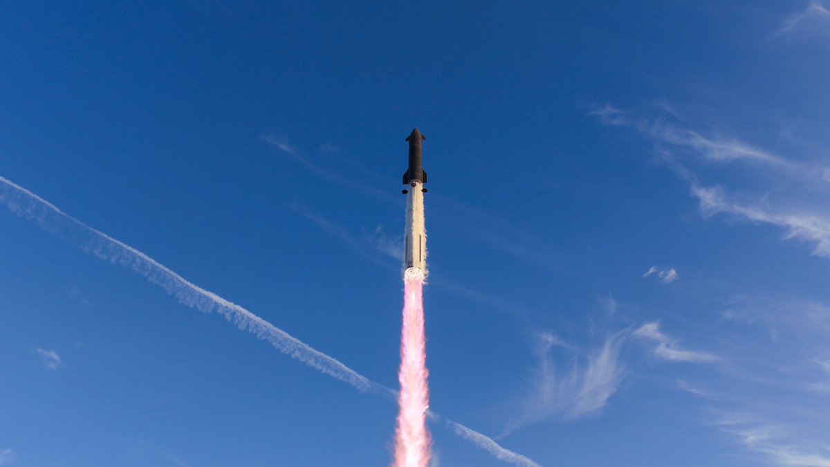

This is how we survive

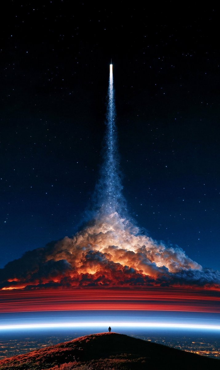

Liftoff of Starship's first orbital flight
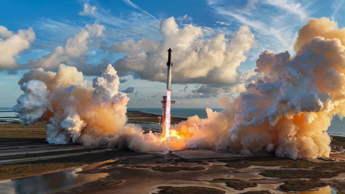


Liftoff of Starship's first orbital flight
TSMC to Stick With Microbumps Over Hybrid Bonding for HBM Packaging for Now, Tasks Suppliers With 5μm Development Taiwan’s TSMC is expected to continue using conventional microbump technology, rather than hybrid bonding, for advanced packaging that connects high-bandwidth memory (HBM) with AI accelerators for the time being. Given the development cycle for related materials, finer-pitch microbumps are expected to remain in use through the later stages of HBM4 and into the early phase of HBM5. According to materials industry sources on September 2, TSMC has asked its materials and equipment partners to develop bonding and underfill solutions for approximately 5-micrometer (μm)-class bumps. In other words, TSMC wants the microbumps currently used in advanced packaging to become even shorter and finer. Korean and Japanese suppliers have begun development, with mass production of 5μm-class bumps estimated to begin in the second half of 2028. Currently, bump heights are approximately 15–25μm for third-generation extended HBM, or HBM3E, while HBM4 is approaching roughly 10μm. Japanese materials suppliers have previously said they have difficulty guaranteeing quality below 15μm. A 5μm bump would therefore fall well below the current qualification threshold. The reason for making the bumps shorter and finer is the height limit of the HBM cube and the need for higher interconnect density. Under JEDEC specifications, the maximum HBM stack height is 775μm. The number of I/O connections continues to increase, but the overall stack must remain within this height limit. In TSMC’s advanced CoWoS packaging, the GPU and the HBM stack—already assembled by the memory supplier—are mounted onto a silicon interposer using microbumps. The stacking of 16 DRAM dies itself is performed within the HBM package by companies such as SK hynix and Samsung Electronics, rather than by TSMC. However, as the number of interconnects on the accelerator side increases, the microbumps used to mount the devices in CoWoS also need to become shorter and more densely packed. First- and second-generation HBM used relatively large solder bumps. As the number of stacked dies and I/O connections increased, microbumps became the mainstream approach around the HBM3 generation. SK hynix has used its MR-MUF process, in which liquid underfill is applied after mass reflow, while Samsung Electronics has used TC-NCF, which places a film-type underfill between the dies before thermocompression bonding. Hybrid bonding has been discussed as the next step. By eliminating bumps and directly bonding copper pads, the interconnect can be made thinner and significantly denser. TSMC already uses this technology, under the SoIC platform, for stacking logic chips. However, HBM is still attached to the interposer using microbumps. The industry has been reluctant to abandon a process that is already proven in terms of yield, inspection, and high-volume manufacturing. At the 5μm scale, manufacturers must simultaneously solve issues involving void-free underfill, residual flux, and bonding alignment. Given the level of difficulty, TSMC appears to have distributed different development tasks across its materials and equipment partners. The direction within the HBM stack itself is similar. At Hot Chips 2026 last month, SK hynix indicated a roadmap under which it would continue using microbump-based MR-MUF through HBM4 and HBM4E, rather than adopting hybrid bonding. Direct bonding was positioned as a technology for HBM5 and for stacks exceeding 20 dies. Industry observers believe JEDEC’s decision to raise the maximum HBM stack height from 720μm to 775μm has provided additional headroom to extend the use of microbumps. A materials industry source said, “TSMC’s request to develop finer microbumps can be interpreted as a signal that, for this generation, it intends to use lower-profile microbumps rather than move to direct bonding.” The source added, “Microbumps below 15μm have already been developed, but guaranteeing their quality remains difficult. The key challenge is not so much the bump itself, but developing an underfill solution that can reliably support and qualify it.”

世界第一CEO搶台灣路人的烤玉米吃 剛剛真實發生 非AI 台灣女網友發文: 在夜市遇到黃仁勳不稀奇 被湊過來問好不好吃,然後手上這隻就⋯ No 我的烤玉米~~~ 真的太有趣太興奮了


記憶體晶片廠商在第一季財報後,對擴張HBM(高頻寬記憶體)產能的態度明顯轉趨保守。 主要原因有三: 一是傳統DRAM(尤其是LPDDR5)目前獲利遠高於HBM; 二是HBM4訂單成長力道略顯疲弱; 三是基於NAND的KV cache記憶體AI推論快速崛起,導致部分原本規劃用於HBM的資本支出,轉向投入傳統DRAM與NAND領域。 此外,晶片廠對簽訂LTA(長期合約)的意願也降低。隨著客戶願意接受每季更高的合約價格,廠商擔心若鎖定長期價格,將錯失供給短缺延續至2027-28年的獲利機會,或在景氣下滑時面臨合約風險。 整體來看,2026下半年至2027上半年,記憶體廠獲利成長將更仰賴傳統記憶體,而非HBM4。新簽LTA長期合約可能趨緩,多數銷售仍以每季議價為主。

BAC: Some chipmakers alluded to reduced interest in LTA (long-term agreement)-based chip sales, given the growing number of customers paying higher DRAM and NAND contract prices each quarter. Chipmakers’ concerns (about LTA) are limited price/profit upside If memory chip supply

AI資料中心引爆光通訊雷射荒,NVIDIA固盤EML重塑供應鏈 TrendForce最新報告指出,AI資料中心大規模叢集化帶動800G以上光收發模組需求暴衝,2025年全球出貨達2400萬支,2026年更飆至6300萬支,年增2.6倍。 需求最上游的雷射光源已成最大瓶頸。NVIDIA為確保Blackwell平台供貨,策略性包下Lumentum、Coherent、Mitsubishi、Sumitomo等主要EML(電吸收調變雷射)廠商產能,交期已排到2027年後,導致市面EML嚴重缺貨。 EML因整合調變功能、製程難度高,全球供應商屈指可數,成為AI長距傳輸關鍵戰略物資。NVIDIA此舉雖穩固自身供應,卻逼非NVIDIA陣營CSP與模組廠加速轉向CW(連續波)雷射+矽光子方案。 CW雷射結構簡單、進入門檻較低,廠商較多,但產能擴充受限於設備交期與後段切割、老化測試,同樣供不應求。 同時,200G高速PD(光二極體)需求同步爆發。因同樣使用InP磊晶,雷射廠優先排產雷射晶片,剩餘InP磊晶產能外溢至台廠iET、全新等專業磊晶廠,迎來顯著訂單。 NVIDIA壟斷EML策略意外加速CW+矽光子技術落地,同時掀起整條光通訊雷射供應鏈產能爭奪戰與格局重組,具高階InP磊晶能力的台廠成為最大受惠者。


歌が上手い人を探しています! 興味のある方、推薦があればDMください!🙇 作品が聴けるURLを添えてもらえると大変助かります🙇 よろしくお願いします🙇
中華人民共和国大使館前、媚中館長陳之漢玉音放送 中华人民共和国大使馆前、舔共馆长陈之汉玉音放送

看到有大哥拋玉! 小弟我做了一個可以自動抓trendforce 每日報價資料的Google sheet(我就懶🥵),有興趣的自行取用! docs.google.com/spreadsheets/d…


. @xXRalphX7
12 Followers 1K Following
夏 @kamochisac62264
475 Followers 6K Following

woman in the wind @woman_wind1
13 Followers 256 Following "AI advocate dreaming of a smarter future powered by artificial intelligence. 🤖
Calista @tigerbana977118
467 Followers 3K Following Ski Dive Fitness Enthusiasts Cryptocurrency Enthusiasts Small Business Owner Holding #BTC ETH XRP🎐🎉
Leonard @Leoskie_L
13K Followers 2K Following AI Semi & Supply Chain | Warsaw × Taiwan Physical layer | US demand ↔ TW supply 100% incremental GM from depreciation expiry Not advice • Just physics.

SpaceX @SpaceX
41.9M Followers 127 Following SpaceX designs, manufactures and launches the world’s most advanced rockets and spacecraft
StatementDog | AI & T... @statementdog
4K Followers 101 Following Tracking the companies and technologies behind the AI buildout. Research informed by company interviews, site visits, analysts, and industry experts.
LIWEI_TW Capital @LIWEI_TWCapital
15K Followers 508 Following Even a great company is only worth recommending at the right price. Every trading idea shared should deliver real, actionable value when it matters most.
Jeff Pu @sssjeffpu
40K Followers 75 Following Tech Enthusiast. 20 years tech equity research + industry.
Simple Tech Trend @simpletechtrend
81 Followers 40 Following ✍️ Editor-in-Chief of Simple Tech Trend 🚀 Decoding Optical Interconnect, CPO, Optical Transceiver, and Silicon Photonics
Gavin Baker @GavinSBaker
357K Followers 6K Following Managing Partner & CIO, @atreidesmgmt. Husband, @l3eckyy. No investment advice, views my own. https://t.co/pFe9KmNu9U

Semi-journal公式 @semi_journal_jp
31K Followers 78 Following 日本最大級の半導体情報サイトhttps://t.co/eEMKNewHQnの公式アカウントです。新着記事・半導体用語・半導体ニュースなどを発信しています。 技術図解は個人アカウントでも投稿中:@semiwan1
Dan Nystedt @dnystedt
55K Followers 1K Following Former journalist, now financial analyst. Based in Taipei. Tweet mainly about semiconductors and Taiwan. Not investment advice. Views are my own.
P Equity Research �... @pequityresearch
65K Followers 935 Following Research 📃 & News 🗞️ | Semis & Tech | Research & Expert Calls: https://t.co/6jzqR9TN4j | China Tech: https://t.co/vptHyJJu79

Palmer Luckey @PalmerLuckey
1.3M Followers 2K Following I am a technology enthusiast, writer, and modder. Founder of @ModRetro, @Oculus VR, and @Anduriltech. Keeping American superheroes safe with autonomous systems.

Ado Staff @ado_staff
331K Followers 14 Following Adoスタッフ公式X💙 niconico https://t.co/VjLSh0DcJQ YouTube https://t.co/CWRnSxY4UQ TikTok https://t.co/aIUSjAXoOQ ご依頼 [email protected] 💌→https://t.co/dfKuvB4XG5
Unclestocknotes @Unclestocknotes
30K Followers 2K Following U.S. stock market influencer | Financial background | Global traveler | Sharing insights on markets, trade, and economics | Swim, basketball, golf enthusiast.
BlueJay @BlueJay87476298
19K Followers 628 Following BASM :哪家公司將成長,進而創造高報酬:經營模式(Business Model)、假設 (Assumptions)、策略 (Strategy)和管理(Management)
魚豊『チ。地球... @uotouoto
93K Followers 553 Following 漫画家 『チ。地球の運動について』https://t.co/BzsdUMlKwg 『ひゃくえむ。』https://t.co/JUnKhteIcp 『ようこそFACTへ』https://t.co/mZPyUoyPeW
劇場版『ゾンビ... @zombielandsaga
197K Followers 89 Following ゾンビィのアイドルは佐賀を、世界を救えるのか―!? 空前絶後のギャラクシー・フェスティバル・ムービー‼ 全国公開中‼ | 2026/5/27(水)Blu-ray発売‼ ▶ハッシュタグ: #ゾンビランドサガ ©劇場版ゾンビランドサガ製作委員会

Black China ブラッ... @superwangbadan
34K Followers 245 Following 日本人中国ウォッチャーです。中国観察歴30年以上。「中国人の民族性と自己愛性人格障害(NPD)の相関性」を研究するため心理学と精神分析学を学ぶ大学生でもあります。心理学から中国人の言動を分析したり、中国時事をネタに漫談する垢です。 #中国人NPD論
台湾史.jp @Formosanhistory
88K Followers 303 Following 台湾屋のひとりごと。台湾の歴史と、そこに隠されたもう一つの日本史(外地史)を探求する歴史探偵…だったのだが、知らぬ間に台湾の森羅万象を扱う総合垢に(笑)街角の「!」を見つける台湾路上探検隊でもあります。中国の話は@superwangbadanでやってます。
咲内ひなた @SakunaiHinata
13K Followers 2K Following Japanese Railfan // デジタル模型鉄 // 川越市出身非ネイティブ日本人 // 中国漢語母語話者(台湾中文・日本語訛り) // 知中派&親台家 // 日台友好一中一台 //多趣味雑多 // 移民政策反対 // 台派・台湾建国派と連帯 // キャラは東津萌米穂姫 // 収益化一切やりません
REiNa @REiNa_017117
2K Followers 215 Following バーチャル界で活動するデジタルシンガーをコンセプトに仮想空間の存在としてYoutubeを中心に活動していますっ⭐️ エレクトロなミドルポップとエモーショナルなオルタナ系ロックが好きです✨フォロー大歓迎っ、お気軽にっ⭐️詳しい活動コンセプトや概要は全てYoutube Channelに記載がありますっ✨
高市早苗 @takaichi_sanae
3.1M Followers 0 Following 衆議院議員 自由民主党奈良県第2選挙区支部長 ※総理在任中の投稿は、一部広報スタッフによるものを含みます。
Ray Wang @rwang07
33K Followers 2K Following Ex-SemiAnalysis "when your motivation runs low, your discipline takes over" “always stay humble, hungry, and curious”
萩森じあ @jirujiaru826
100K Followers 987 Following 絵を描きます【お仕事はこちらに✉️[email protected] 】◆画集発売中です→ https://t.co/MXDV2BLlv1 ◆MV https://t.co/bFXFXnoXjQ ◆インスタ https://t.co/4yrxbJxTWj
Shiro AI @shiro_ai_jp
1K Followers 59 Following 日本のAIを使ったクリエイター。こちらでは自慢をしたり溜まっていたログを吐いたりします🍣 Creative Partner: Vidu,Hailuo
SBG @SBG_jerry_1006
2K Followers 1K Following Ion trap researcher~~轉行到半導體~希望能工程鼠的角度觀察產業 最近的產業topic:AP(先進封裝 : Cowos、glass core、hybrid bonding、soft X Ray inspection )、 Si-ph(矽光子)、embedded cap、IVR
TrendForce @trendforce
24K Followers 658 Following Founded in 2000, TrendForce is a global provider of market intelligence on technology industries based in Taipei. Also find us on https://t.co/FHEud9jhQd
股海飯桶🍚 wils... @stockwilsonrice
6K Followers 77 Following 食量太大,為了養活自己所以開始投資,這邊分享產業研究員日常、投資心得以及如何辛苦的養活自己😓,歡迎大家交流~ [email protected]

nowisee @nowisee_jp
5K Followers 9 Following - 視覚と聴覚の両方を刺激させる正体不明のクリエイター集団 - 「外見や実績に囚われず、鳴らす音楽の力で勝負したい」 という思いから匿名性を貫き通しているため各メンバーの素性は明かしていないが 1 人の女性ボーカリストと 5 人の男性クリエイターの 6 名で各分野のプロフェッショナルとして活動しているユニット。
ろん / LON @LOOON4
241K Followers 83 Following 野菜ジュースは世界を救う HP▸https://t.co/bfOMRWAfaG 地下室▸https://t.co/ig2xhUkaoz ニコニコ▸https://t.co/LptJ1Ptk9g mail▸[email protected] とりさん@LON_puku
ゆってぃ💍︎�... @yukina__0069
265K Followers 11 Following 人妻ゆきなです💍軽率に呟いていくね✌️フォローしてくれてる人ガチ勢すぎて大好きなので認知していく✌️✌️✌️本垢もフォローしてね@yukina0069

The White House @WhiteHouse
5.3M Followers 5 Following Welcome to The Golden Age of America. 📱 Text USA to 45470 to receive alerts.
Donald J. Trump @realDonaldTrump
111.8M Followers 53 Following 45th & 47th President of the United States of America🇺🇸
游庭皓的財經皓... @youtinghao
6K Followers 0 Following 游庭皓,90後,財經作家、投資人。清華大學經濟學學士,台灣大學法學碩士,曾任投資顧問公司研究員、經濟日報、聯合晚報、Yahoo財經撰稿人、台灣財經節目特邀來賓,研究方向以總體經濟變化與景氣宏觀投資為主。

股海小水手 Stron... @CURARPIKTchu
7K Followers 49 Following talking something interesting about investment

TrendForce Japan @TrendForceJP
2K Followers 19 Following TrendForceは市場調査会社であり、グローバルハイテク市場を分析しています。私たちはメモリ、AIサーバー、HBM、半導体、ファウンドリ、ディスプレイ、LED、MLCC、中国EVなどの情報を提供し、『意思決定科学』を行い、企業の成長を支援する信頼できるパートナーを目指しています。
ゆある @yu_nk3
27K Followers 325 Following @yuarigoto #ゆあるみて 🧸 https://t.co/d7iEa6m0hk 📩 [email protected]
ケンモチヒデフ... @h_kenmochi
32K Followers 2K Following Sound producer , DJ, 作詞作曲編曲家。水曜日のカンパネラの音楽担当。他いろいろ手広く音楽作ってます。ソロではシカゴフットワークなども。 [email protected]
水曜日のカンパ... @wed_camp
90K Followers 3K Following 水曜日のカンパネラのオフィシャルX。Dir.Fとスタッフがつぶやいてます【メンバー】主演&歌唱:@utaha_89_id_、音楽:@h_kenmochi、その他:Dir.F E-mail→[email protected] 曲の感想見つけてたまに「いいね!」してます

ogasawara_yoshiyuki @ogasawara_yoshi
4K Followers 308 Following Researcher on the Taiwanese Politics, Elections, and Taiwan-China relations. Visiting Professor at National Tsing Hua University (Taiwan). 台湾政治,総統選挙,中台関係
Trends for United States
You might like